The right bonding technology -
adaptable in every process step

Choosing the right bonding technology makes the difference. It depends on your materials, device design and functional requirements, and must also match your production volume and reliability needs.

Our systems support all major die bonding technologies and enable you to adapt or switch bonding approaches within a process or between processes as your devices or production requirements evolve.

Optimize every step: Adjust bonding methods dynamically within a process
Select the right technology: Tailored to each application and device
Future-proof your device: Change bonding strategies without rebuilding workflows
Three researchers standing in front of a FINEPLACER Femto 2, looking at the screen while an active process is being configured.

Ultrasonic bonding

This bonding technology is mainly used for flip chip applications to create mechanically and electrically stable connections. It is a friction welding process that attaches a chip to a substrate without additional joining materials, using pressure and ultrasonic energy to initiate diffusion between contact areas. The bonding process occurs within milliseconds.

Ultrasonic die bonding is well suited for applications with limited heat tolerance or where joining materials such as solder or adhesives cannot be used.

Read the technical paper

Thermocompression bonding

A bonding method that forms reliable interconnections through the application of pressure and elevated temperature, primarily used for flip-chip die bonding.

In this context, thermocompression bonding refers to processes based on gold stud bumps or indium bumps, delivering high mechanical strength and stable electrical performance for advanced electronic and photonic applications.

Read the technical paper

Indium bump interconnect flip chip bonding

This bonding method enables high-density interconnects for advanced devices such as FPA imaging sensors, IR detectors, quantum processors, and microLED displays. Increasing pixel and qubit counts and larger die sizes drive the need for fine-pitch interconnects and sub-micron alignment accuracy.

Sensitive materials, mismatched CTEs, and extreme operating conditions—such as cryogenic environments—limit the use of high-temperature or chemically assisted bonding processes. IBI bonding enables precise, low-temperature flip-chip interconnection, making it a key bonding method for next-generation heterogeneous integration.

Read the technical paper

Adhesive bonding / UV curing

A die bonding method that forms mechanical and, if required, electrical connections using polymeric or epoxy-based adhesives, typically cured by heat or UV exposure.

This bonding approach enables low-temperature processing, accommodates material mismatches, and provides flexible integration options for electronic and photonic applications where thermal or mechanical constraints are critical.

Read the technical paper

Eutectic bonding

This is a die bonding method that creates strong mechanical and electrical connections by forming a eutectic alloy at the interface between the die and substrate through controlled temperature.

This bonding technique provides excellent thermal and electrical conductivity, precise bond line control, and high long-term reliability for demanding electronic and photonic applications.

Read the technical paper

Laser assisted bonding

Suitable for C2S and C2W applications with high requirements for process speed, accuracy, and precisely controlled local heat input, even in very small areas. Rapid temperature cycles minimize surface oxidation, shorten process times, and ensure that each chip is heated only once during substrate- or wafer-level bonding.

Unlike area heating, localized laser heating avoids thermal expansion challenges, allows chip spacing as low as 500 µm, and reliably protects adjacent solder joints from re-melting.

Read the technical paper
Finetech die bonders can be configured to integrate all relevant bonding methods within one modular platform. This allows complex assemblies and heterogeneous integration workflows to run on a single system with consistent accuracy and process control.

Hybrid bonding for 2.5D & 3D Packaging

Hybrid bonding enables direct electrical and mechanical connections between dies at extremely fine pitches, supporting advanced 2.5D and 3D packaging architectures. By combining direct die-to-die or die-to-wafer bonding with ultra-fine interconnect density, hybrid bonding overcomes the limitations of conventional packaging approaches.

This method improves signal integrity, power efficiency, and thermal performance while enabling higher levels of integration and reduced form factors. Achieving reliable hybrid bonding requires high alignment accuracy and precise process control to assemble high-density dies with large interconnect counts.

Read the technical paper

Heterogeneous Integration through Advanced Bonding

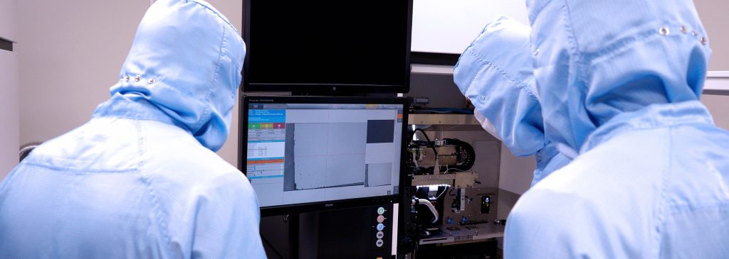
Heterogeneous integration enables the co-integration of dies from different process nodes, materials, and functions, allowing flexible architectures that balance performance, power efficiency, and cost. This level of integration is enabled by the combination of advanced bonding methods, selected and optimized to support high-density, low-loss interconnects across diverse technologies.

Reliable implementation requires precise alignment and controlled assembly processes to ensure consistent electrical, thermal, and mechanical performance while maintaining yield across mixed-technology components.

Read the technical paper

One Platform. Multiple Bonding Technologies.

Contact Us

If you have a service request, please click here.

このフィールドは必須です。
このフィールドは必須です。
このフィールドは必須です。
このフィールドは必須です。
このフィールドは必須です。
このフィールドは必須です。
このフィールドは必須です。
このフィールドは必須です。
このフィールドは必須です。
このフィールドは必須です。
このフィールドは必須です。
このフィールドは必須です。
このフィールドは必須です。
このフィールドは必須です。
このフィールドは必須です。
このフィールドは必須です。
このフィールドは必須です。
このフィールドは必須です。
このフィールドは必須です。
このフィールドは必須です。