As part of the co-operative project “Silicon Photonics Enabling Exascale Data Networks (SPEED)”, Finetech handles the experimental assembly of innovative silicon photonics based 4-wavelenghts- 400 GB/s-transceivers with direct detection.
Digital information is an essential part of our life. The exponentially growing amount of transmitted data is a key challenge in the development of future-proof data networks. Society’s demand to provide more bandwidth for all subscribers is accounted for by developing increasingly powerful network components.
In light of these requirements, the Federal Ministry of Education & Research is funding the project „Silicon Photonics Enabling Exascale Data Networks (SPEED)”. Bringing together numerous German research institutes and component manufacturers, main goal is the development of high-bit-rate optical transceiver modules as an essential part of future waveguide based networks. The board-mount optical transmitter and receiver modules allow highest transmission rates for data transfer between data centers.
Key objective is the development of two 400 Gb/s transceiver module for various areas of application. One is a four wavelength direct-detect solution for intra-data center, while the other is a single-wavelength tunable coherent device for inter-data center interconnects.
Both modules will be designed based on innovative silicon photonics. This forward-looking technology is already playing a big part in modern communications electronics and is increasingly common on the market.
The innovative approach pursued by the SPEED consortium will help the industry tackle critical issues concerning cost efficiency, power consumption and thermal management. Moreover, the project is to lay the foundations of an entire value chain for innovative transceiver modules made in Germany.
FINEPLACER® Bonders to Handle Challenging Assembly Tasks
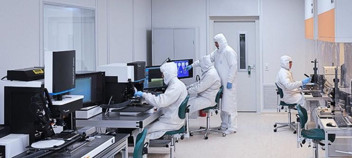
A major challenge in building the modules is engineering an assembly process to adjust the laser at a defined angle. To this date, this could only be realized with complex calculations leading to a fixed machine configuration provided by the system manufacturer. The alternative was a fully-automatic flip chip bonder. However, especially for small and medium-sized companies, investing in an advanced fully-automated bonding system is a big financial commitment and a venture that is often difficult to assess. Therefore, an explicit sub goal of SPEED is to realize assembly solutions specifically suited for laboratory bonders to make it easier for start-up and smaller companies to enter this new market segment.
With long-term experience in manufacturing manual and semi-automated R&D bonders and a profound knowledge of how to develop new applications and technologies, Finetech is a natural partner of the SPEED consortium.
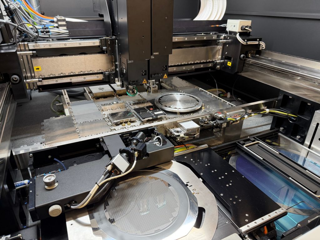
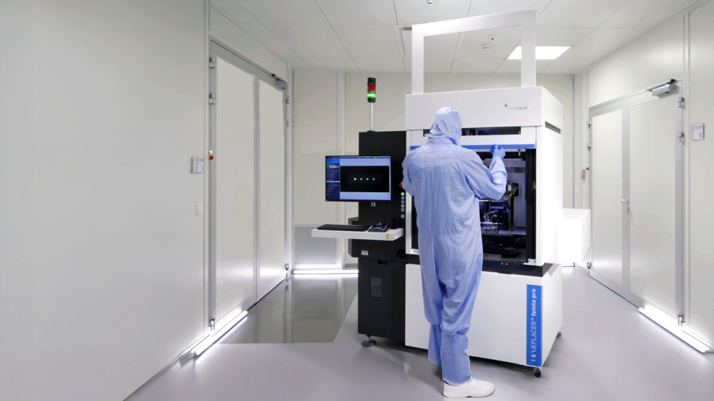
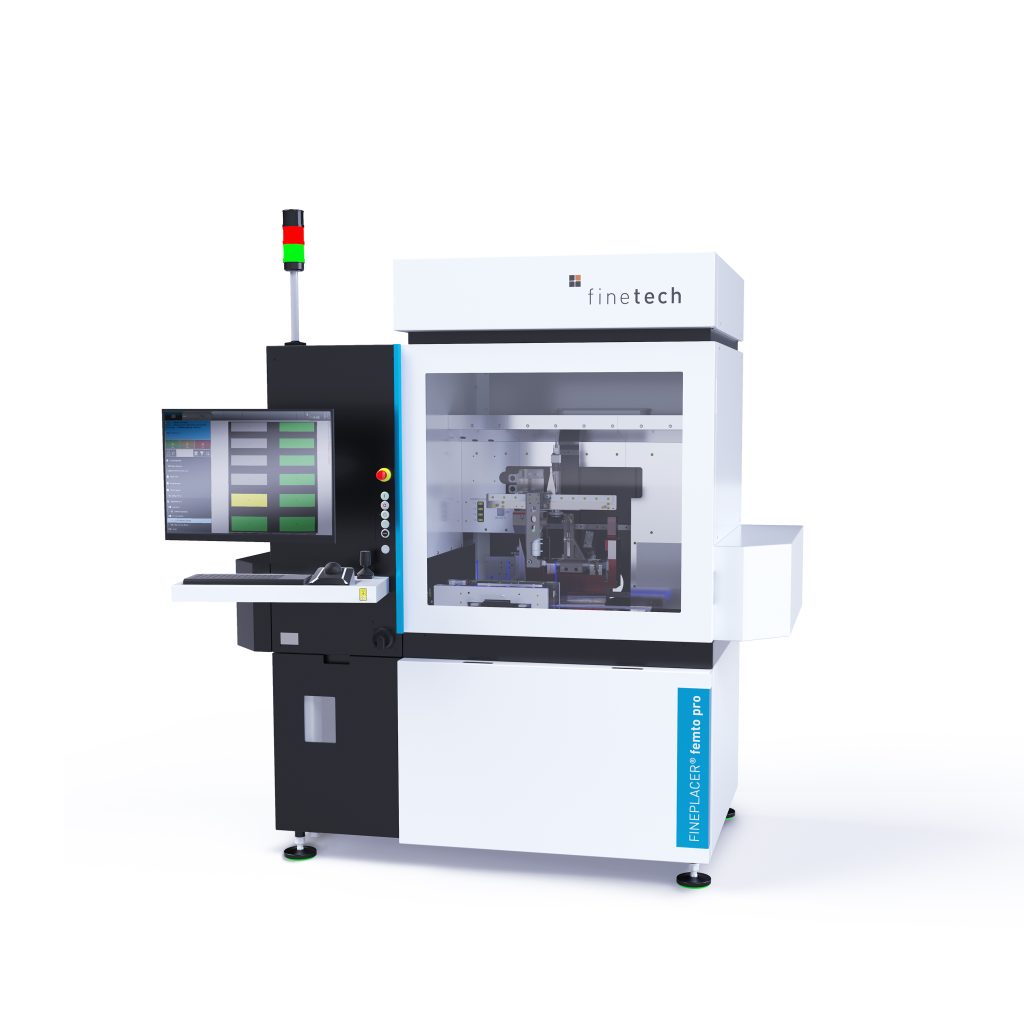
The semi-automated customizable die bonders support a variety of sub-micron assembly technologies and provide optimal conditions for the assembly of experimental demonstrator samples of the innovative transceiver modules.
The patented FINEPLACER® alignment and placement principle suits the assembly of a wide spectrum of components and submodules from various industries, such as medical technology, precision mechanics, sensor assembly, solar technology for high power lasers, mini displays or nano technology.
The FINEPLACER® bonder’s modular system architecture supports the future-proof retrofit of new technologies and flexible machine configurations adaptive to changing requirements.

