
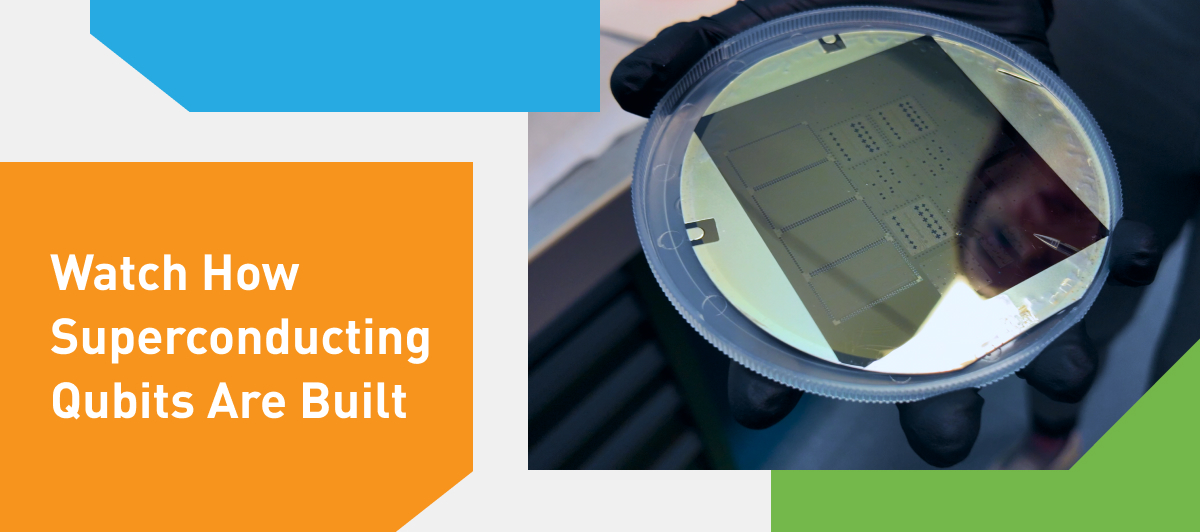
// Watch How Superconducting Qubits Get Built

There is one moment every superconducting qubit team waits for. The processor sits in the cryostat at around 10 millikelvin, the first microwave signals go in, and everyone watches the data. 

We spent a day with Peak Quantum and the Walther-Meißner-Institut (WMI), following their processors from the cleanroom to the cryostat. On the way: the advanced packaging step that decides how that moment ends. 

The Film: From Cleanroom to Cryostat

In this video, experts from Peak Quantum, the Walther-Meißner-Institut (WMI) and Finetech show how superconducting qubits are made and bonded on the FINEPLACER® femto 2, and what matters most along the way. A research institute, a quantum start-up, and the equipment and solution provider behind their bonding process. 

Signals for Every Qubit

Essentially, you need to attach one wire that is the size of a hair to each of the qubits.”

Leon Koch
Co-founder, Peak Quantum

For Peak Quantum, this is the biggest bottleneck on the way to a fault-tolerant quantum computer. Its new architecture builds error protection into the hardware and needs an order of magnitude fewer physical qubits. But every qubit still needs its signal line. 

In research, those lines come in from the side. At scale, they have to come from the top. That makes the processor an advanced packaging problem: qubit chip and control chip, stacked and flip-chip bonded through indium bump interconnects (IBI). 

In the Cleanroom: Everything Leads to the Bond

By the time the chips reach the cleanroom, most of the fabrication is done. Superconducting material has been deposited on the wafer and patterned by lithography, Josephson junctions included. Indium bumps have been evaporated on at wafer level, and the wafer has been diced into chips. 

In the cleanroom, the chips are chemically cleaned and prepared for bonding. The bond is the last step before the fridge and carries all the work that came before. 

"If it fails, the quantum processor will not function."

placeholder_image
Léa Richard
Walther-Meißner-Institute
wmi-ibi
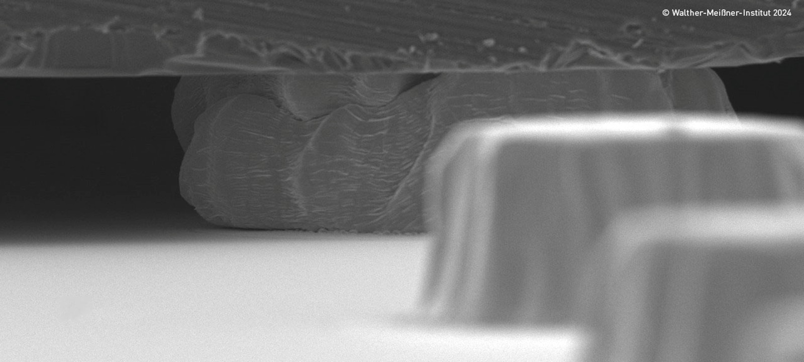
Indium bumps carry the signal between the stacked layers of a superconducting quantum processor.

At the Bonder: Precision, Contact Quality, Process Control

“The contact quality and the placement accuracy of the qubit chip on the readout chip directly impacts the performance of the final quantum computer.”

Travis Scott
Finetech
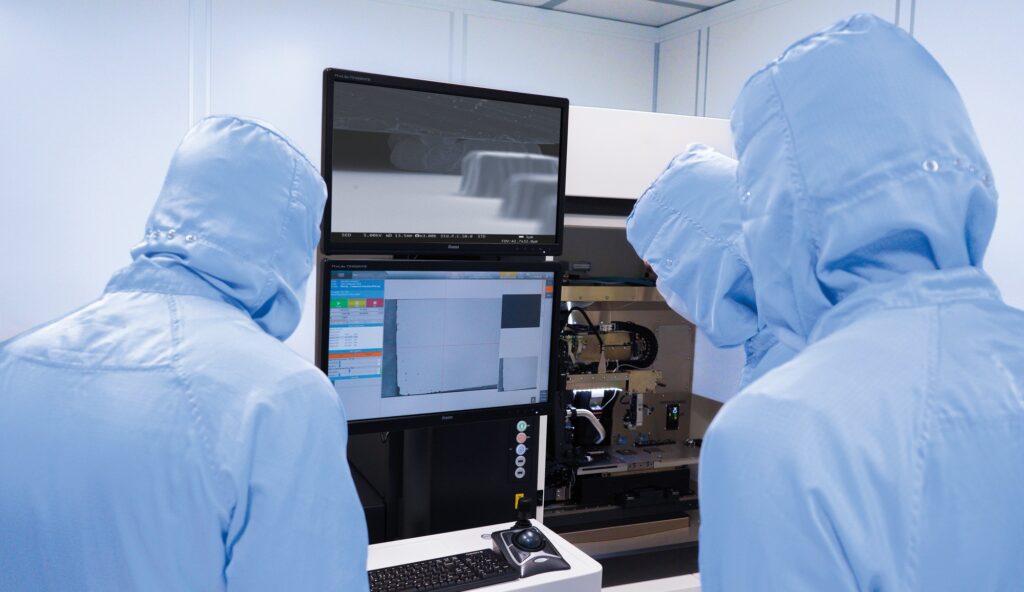
In a quantum processor, the gap between the two chips is part of the circuit. The process has to control: 

  • the vacuum gap, through indium bump compression 
  • X/Y alignment at sub-micron accuracy 
  • co-planarity and bond line thickness, identical from chip to chip 
  • temperature and process gas, such as formic acid for oxide reduction 

On the FINEPLACER® femto 2, Finetech runs this as one standardized IBI process. Interconnect yields reach above 99%, stable under repeated cryogenic cycling. 

Before the chip moves on, an infrared microscope checks the alignment and a resistance measurement confirms the connection. 

Flip-chip bonding of a superconducting qubit stack on the FINEPLACER® femto 2.

In the Cryostat: The Moment of Truth

“There's always a moment of tension, because all the work […] comes down to this moment.”
placeholder_image
Diego Esteban Contreras de Abreu
Peak Quantum

The processor is packaged and cooled to around 10 millikelvin. Microwave signals show how long the qubits hold their state and how well they can be controlled. 

A bond that is off shows up immediately: higher losses, shifted frequencies, states that decay too fast. That makes this measurement the final quality test for every step before it, flip-chip bonding included. 

A clear qubit signal means the whole chain worked. The data goes straight back into the next design. 

From Demo Trial to Pilot Line

“The only axis left for scaling is a vertical stack.”
Travis Scott
Finetech

The collaboration goes back years. WMI first came to Finetech in Berlin for demo trials at a very early stage of its 3D integration work. Today it builds its processors with cold-compression IBI on its own FINEPLACER® femto 2. Peak Quantum, founded out of WMI, has its processors bonded there, on the same system. 

Both are partners in SUPREME, the European Chips Act pilot line for superconducting quantum circuits. One milestone: a 200-qubit 3D-integrated module. In September 2026, the BMFTR also selected ATHENA-X, led by Peak Quantum with WMI, to build an error-corrected quantum computer. 

Every processor on the way to that 200-qubit module will face the same moment in the cryostat. Whether it ends with a clear signal is decided earlier, in advanced packaging.  

Building superconducting qubits or moving to 3D integration? Get in touch with our team. 

Contact Us

関連情報

Contact Us

このフィールドは必須です。
このフィールドは必須です。
このフィールドは必須です。
このフィールドは必須です。
このフィールドは必須です。
このフィールドは必須です。
このフィールドは必須です。
このフィールドは必須です。
このフィールドは必須です。
このフィールドは必須です。
このフィールドは必須です。
このフィールドは必須です。
このフィールドは必須です。