2nmプロセスで製造され、テストにも合格し完全に動作するチップが、廃棄箱へと放り込まれる場合があります。シリコン(半導体そのもの)が欠陥品だったからではありません。それを取り囲む「パッケージング」が失敗したためです。
これが、シリコンフォトニクスが直面している冷徹な現実です。フォトニクス・チップが最終的な「製品」へと昇華できるかどうかを決めるのは、もはやデバイスそのものの性能ではありません。パッケージング(実装技術)こそが、すべてを左右するのです。
このパラダイムシフトは、AIの台頭によって猛烈なスピードで進行しています。データセンターは、現在のインターコネクト(相互接続技術)の限界を超える帯域幅(バンド幅)、低遅延(レイテンシ)、および低消費電力を求めており、シリコンフォトニクスはその要求に応えられる数少ない有力な解決策の一つです。しかし、動作するデバイスを「数百万規模の信頼性の高い製品」へと量産展開できるかどうかは、リソグラフィ(露光技術)ではなく、アセンブリ、高精度アライメント、そして接合(ボンディング)プロセスにかかっています。業界が長年を費やして前工程(フロントエンド)を洗練させてきた結果、現在のボトルネックは完全に後工程(バックエンド)へと移行しています。
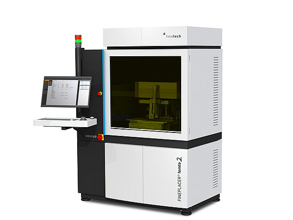
ここで、設計(デザイン)を量産化(プロダクション)へと導く決定的な役割を果たすのが、超精密なダイボンディング技術です。光学特性、電気信号の品質(シグナル・インテグリティ)、熱挙動、および機械的安定性、これらはすべて、パッケージがいかに正確にアセンブリされ、そのプロセスが量産時にどれだけ安定して再現できるかにかかっています。Finetechは、まさにこの重要な分岐点となるボンディングシステムを構築しており、シリコンフォトニクスの量産化を推し進める最先端の開発者たちと長年にわたり緊密に連携してきました。本記事では、この領域における真の課題と、それを突破するために必要なアプローチを紐解きます。
パッケージが製品そのものになった理由
従来の電子機器において、パッケージングは最終工程に過ぎませんでした。デバイスを保護し、外部の世界と接続するためのものであり、コストが重視される単なる組み立てステップとして扱われていたのです。
しかし、シリコンフォトニクスはそのモデルを根底から覆します。現在のパッケージングは、以下の4つの役割を同時に果たさなければなりません。
- ライトガイド(光軸の整合)
- 高速電気信号の維持
- 熱管理(放熱制御)
- 長期運用における、極めて精密な位置関係にある異種材料のポジション維持
わずかな位置ズレであっても、光結合効率や信号品質、そして長期信頼性は著しく低下します。これこそが、シリコンフォトニクスにおいて、パッケージングが最終的な製品価値の大部分を占め、場合によってはチップ自体のコストに匹敵することがある理由です。この現実により、企業はプロセス開発、製造装置、そしてサプライチェーンの準備状況を根本から再考せざるを得なくなっています。
ダイ・ツー・ウェーハ(Die-to-Wafer)ボンディング、チップレットインテグレーション、インターポーザ、ハイブリッド・ボンディング、そして異種材料統合(ヘテロジニアス・インテグレーション) といった技術は、パッケージングをウェーハレベル製造の領域へと引き上げています。これらはもはや、従来のような「後工程の組み立て作業」ではありません。クリーンルームに対応したプロセス、正確な配置(プレースメント)、そして安定した再現性のある接合が絶対条件となるのです。
FinetechのセールスマネージャーであるSylvain Dulphyは次のように指摘します。「パッケージングに不備があれば、製品全体が失われます。内部の2ナノメートル・チップがいかに高品質であろうとも、パッケージングが完璧に実現されなければ、そのユニットは廃棄されるしかないのです」
スイッチ部で限界を迎えるプラガブル・モジュール
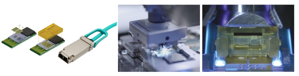
これまでプラガブル(着脱型)光モジュールは業界に大きく貢献してきました。しかし、データセンターの高速化・高密度化が進むにつれ、消費電力、シグナル・インテグリティ(電気信号品質)、および物理的な距離の制御が極めて困難になっています。現在、銅配線(電気)と光ファイバー(光)の世界は融合しつつあり、これこそが「CPO:Co-Packaged Optics」が急速に台頭している理由です。光エンジンをスイッチASICやプロセッサの近くに配置することで、信号が光に変換される前の電気的な経路(パス)を短縮できます。超高速の領域では、このわずかな物理的距離がシステム全体のパフォーマンスに直接影響を及ぼします。しかし、ここで問題となるのは、この「より短く、より高密度な接続」こそが、量産時に最も正確な搭載(プレースメント)を困難にするという点です。
Dulphy曰く「電気信号の経路が長すぎると、その経路自体が実質的に『フィルター』として機能してしまい、信号を減衰させてしまいます。例えどれほど処理速度を高めても、接続距離によって信号強度が低下してしまえば、システム全体のパフォーマンスに制約(キャップ)がかかってしまうのです」
接続は、より短く、より高密度に、そしてよりダイレクトに行われなければなりません。この要求が、バンプ、インターポーザ、金属間(Metal-to-Metal)接合、チップレット、および3D積層アーキテクチャへと設計を推し進める要因となっています。
そして、難易度はさらに複合化していきます:
- 光学機能と電気機能が1つのパッケージに共存する
- 熱膨張係数(CTE)の異なる材料同士の混載
- 極限までの機械的な許容誤差(公差)の最小化
- アセンブリ工程中だけでなく製品寿命期間の全てにわたる正確な位置の維持
量産における手動アライメントの課題
光学アライメント(光軸調整)は、シリコンフォトニクス・パッケージングにおいて最も困難な工程の一つです。
現在でも多くのアプリケーションでは、この調整が「アクティブ・アライメント」によって行われています。そのプロセスは、ファイバーやレンズなどの光学素子を配置し、レーザーを実際に点灯させ、信号強度を測定しながら位置を微調整し、最適な光結合効率が得られるまで微調整を繰り返す、というものです。
この手法は非常に高精度であり、技術的にも確立されています。しかし、量産フェーズにおいては、処理速度が遅く、極めて高コストな要因となります。
そのため、より高い生産ボリュームを求める業界では、「パッシブ・アライメント」へとシフトしつつあります。機械的な基準(メカニカル・リファレンス)や中間光学構造、そして再現性の高い搭載精度(プレースメント精度)を活用することにより、すべてのユニットを「アクティブにして」最適化を行う必要性を低減させています。
しかし、パッシブ・アライメントを採用したからといって、課題そのものが消失するわけではありません。難易度がプロセスチェーンの他の部分へと移行するだけです。基板、光学素子、接合精度、熱挙動、および検査を含むすべてを完璧に整合させる必要があります。つまり、開発・試作段階で上手くいったコンセプトであっても、その「パフォーマンス・ウィンドウ(要求仕様を満たす許容範囲)」を維持したまま量産ラインへと移行できることが実証されなければならないのです。
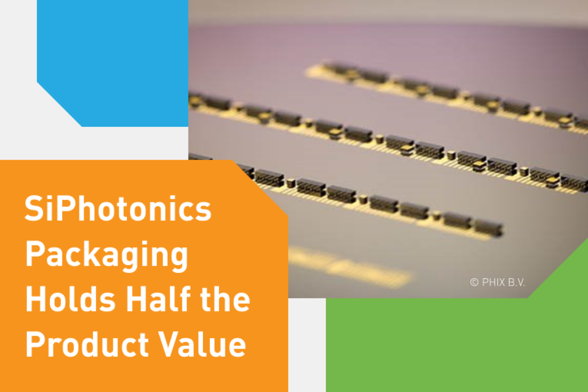
VCSEL、フォトダイオードアレイ、およびサーミスタが実装されたSiN(窒化ケイ素)フォトニック・ウェーハ。ウェーハを正常に機能する製品へと仕上げるには、これらアクティブコンポーネントの極めて精密なアセンブリが必要です。 (© PHIX B.V.)
標準化も製造装置も未成熟な中、近道はない
量産化(スケーリング)における課題は、構造的なものです。シリコンフォトニクス・パッケージングにおいては、業界全体で広く受け入れられている標準規格(スタンダード)が未だ確立されていません。各企業がそれぞれ独自のアーキテクチャ、インターフェース、およびプロセスフローを構築しています。これは技術革新のスピードが速い分野においては理解できることですが、業界全体としての知見の蓄積や学習スピードを鈍らせる要因となっています。
また、製造装置も制約となっています。従来の一般的なアセンブリ装置は、そもそもこうした用途を想定して設計されていません。この領域で求められるシステムは、以下のような複数の高度な機能を1つのプラットフォームに統合している必要があります。
- 高い搭載精度(プレースメント精度)
- 異種材料のミキシング・ハンドリング
- 光学および電気インターフェースの融合
- 3Dアライメント(立体的な位置決め)
- プロセスのトレーサビリティ
生産における高い再現性
アプリケーションが成熟するのを待ち、その後に生産システムを適応させようとするのは良い選択ではありません。製造装置の開発とプロセスの開発は、常に「二人三脚」で同時に進められなければなりません。
この現実は、すでに企業の業態のあり方を変貌させつつあります。ファウンドリは先進的なインテグレーション機能の拡張を進め、前工程(フロントエンド)のプレイヤーはパッケージング領域へと深く踏み込み、装置サプライヤーはより早い段階からアプリケーション開発に巻き込まれるようになっています。今や、研究機関、システムインテグレーター、そしてパッケージングの専門家が同じテーブルについて開発を進める時代が到来しているのです。
ダイボンディングは量産移行への分岐点
シリコンフォトニクスにおける多くのプロセスは、研究室(ラボ)の中ではなく、量産(プロダクション)へのハンドオーバー(引き継ぎ)の段階で失敗を迎えます。開発プラットフォーム上で機能したボンディングのレシピであっても、スループット(処理速度)、歩留まり、およびトレーサビリティが製品の成否を決める量産ラインへと移行し、そこで通用しなければ意味がありません。が真価を発揮するのは、まさにこの「ハンドオーバー」の領域です。
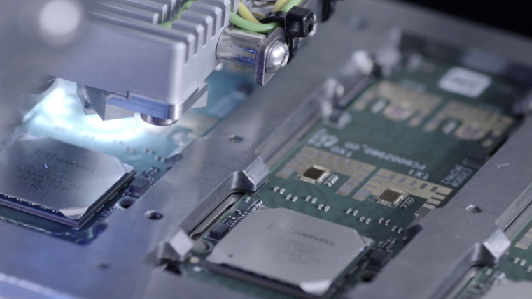
超精密ダイボンディングは、製品の成否を分ける決定的なステップです。高い搭載精度、精密に制御された荷重(ボンディングフォース)と温度、そして1つのプロセス内で異なる材料を処理できる柔軟性こそが、「見栄えの良いプロトタイプ」と「商業的に製造可能な製品」を隔てる境界線となります。 一例を挙げると、ウィーン工科大学(TU Wien)の研究グループは、Finetechのボンダーを使用して、III-V 族テラヘルツ・量子カスケードレーザーをシリコン上へダイレクトにフリップチップ実装 することに成功しました。これにより、電気的コンタクト(導通)が可能になっただけでなく、レーザーの熱特性(放熱性)が劇的に向上しました。Finetechはまさにこれらの要求を満たすシステムを構築しており、初期のフィージビリティスタディ(実現可能性検証)から再現性のある量産に至るまでお客様をサポートしているため、開発の初期段階で構築したプロセスを後からゼロから再開発する必要がありません。
また、同様の要求は、フォトニクス領域を超えて、量子技術、MEMS、体内埋め込み型医療電子機器、および高度なセンサー分野でも見られます。共通しているのは、許容誤差が極めて厳しく、エラーが一切許されない環境下で、高付加価値なコンポーネントをアセンブリするという点です。いずれのケースにおいても、ボンディングプロセスは製品性能、歩留まり、および量産展開(スケーラビリティ)に直結しています。だからこそ、接合技術は開発の「最後」ではなく、設計の「最初」の段階から議論されるべき重要なテーマなのです。
動作するデバイスから出荷可能な製品へ
シリコンフォトニクスは、次世代のAIインフラストラクチャ、高速ネットワーキング、および高度なセンシング領域において明確な地位を確立しています。しかし、市場へ普及するためには、優れたデバイス設計(デザイン)だけでは不十分です。
業界では、以下の要素をすべて同時に成立させる必要があります。
- 確立されたパッケージングの標準規格
- 量産展開が可能な(スケーラブルな)アライメント戦略
- 量産に対応できるボンディング(接合)技術
- アプリケーションと並行して開発される製造装置
- ファウンドリ、装置メーカー、研究機関、システムインテグレーター、およびパッケージングの専門家間の緊密な協力体制
すでに、AIデータセンター、CPO(co-packaged optics)、ハイパフォーマンス・コンピューティング(HPC)、および高度に統合された光電融合(フォトニック・エレクトロニック)システムを中心に需要は形成されています。次のフェーズへと進めるかどうかは、サプライチェーンがいかに迅速に、有望なデバイスを「スケールメリットの効く量産製品」へと転換できるかどうかにかかっています。
廃棄箱に入れられた2nmチップは、業界への警鐘です。それらはすべて、安定維持できなかった製造プロセスによって失われた「正常に動作していたはずのデバイス」なのです。シリコンフォトニクスを量産化(ボリューム生産)へと導くということは、このような損失を完全に食い止めることに他なりません。
※本記事は、Silicon Semiconductor Issue V 2026に掲載されたSylvain Dulphyの特集記事を元に構成されています