The assembly of complex 2.5D and 3D IC packages requires the highest placement accuracy. If these packages are being placed to wafers, the same accuracy must be preserved but across the entire surface of large substrates. Up until now, this has been difficult to do.
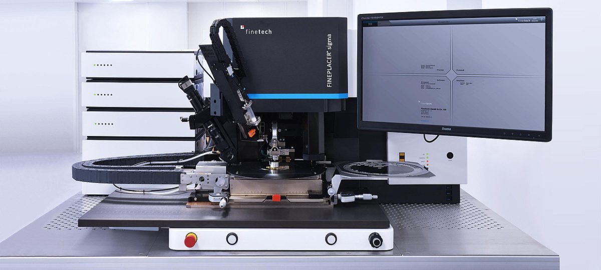
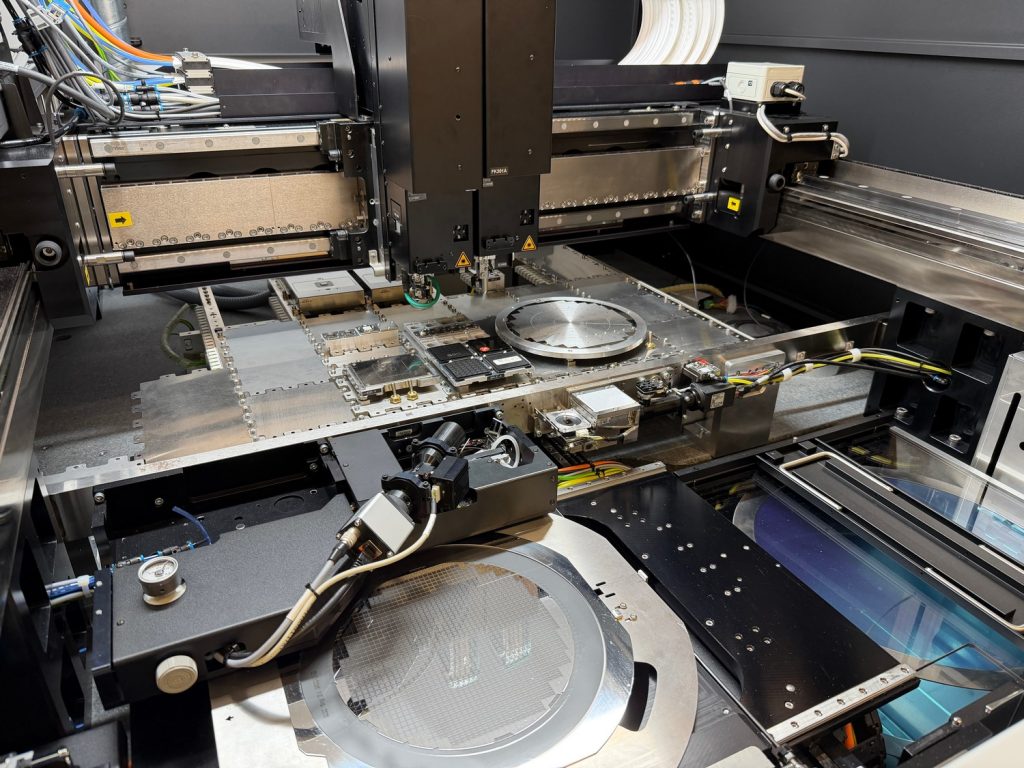
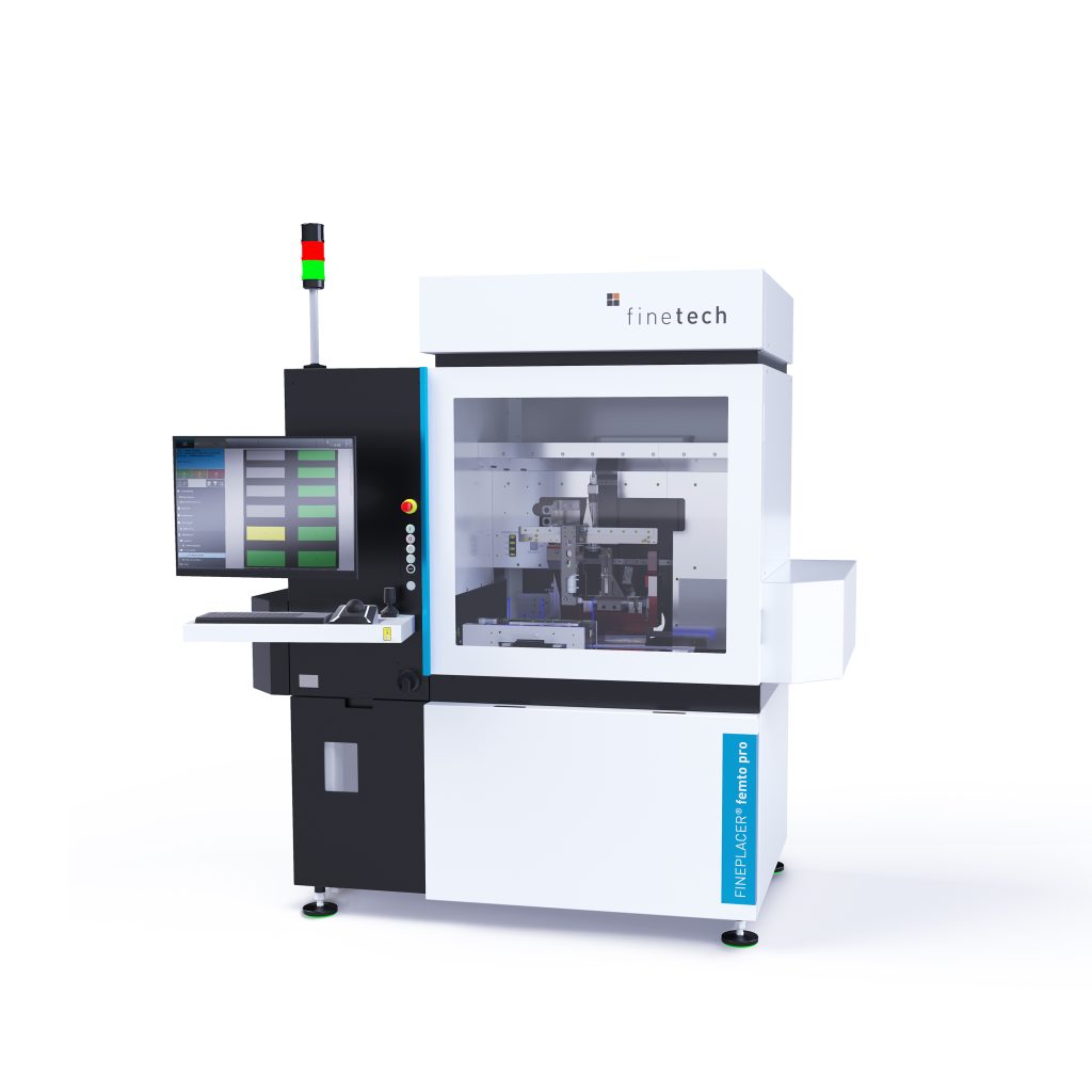
The all-new die bonding platform FINEPLACER® sigma offers this capability. The system combines sub-micron placement accuracy with a spacious working area suitable for substrates up to 450 x 300 mm². Also, the bonder is equipped to support bonding forces up to 1000N which makes it the ideal choice for all kinds of Wafer Level Packaging (FOWLP, W2W, C2W) used to assemble MEMS/MOEMS, IR/ image sensors and all kinds of precision high I/O count applications.
FPXvisionTM – the New Generation of Finetech’s Vision Alignment System
The centerpiece feature of the FINEPLACER® sigma is the newly developed Vision Alignment System FPXvisionTM, taking Finetech’s well-proven FINEPLACER® principle of swivel arm and overlay image to the next level. Two stationary high definition cameras provide the video feeds used for the overlay image, and specially developed optics ensure that the cameras’ full resolution potential is tapped.
FPXvisionTM provides highest resolution at all magnification levels and real-time optimized camera images. This enables excellent and uniform representation of smallest structures across the whole surface, even with particularly large components and substrates.
As a first, the new Vision Alignment System introduces pattern recognition to a die bonding platform with manual alignment. When aligning chip to substrate, the OPR provides precise position feedback to allow for a very easy software-assisted alignment process. This approach ensures a reliably precise alignment process due to minimized operator influence
Furthermore, various illumination options allow more freedom when working with different component/substrate materials and surfaces.
Intuitive Process Management with IPMCommand
The operating software IPMCommand has been fundamentally revamped and offers comprehensive creation and modification options for every aspect of the process. The well-organized program structure and consistent, simple user interface deliver a hassle-free process.
The entire process management is software-based and can be optionally controlled by touch operation. Each process parameter can be modified by the tap of a finger. The interaction via well-established multi-touch gestures, such as pinch-to-zoom, is supported.
Working with customers during the evaluation stage, the winning combination of comprehensive functional range and user friendly operation was met with great approval.
Technological Diversity and Future Viability
As a future-proof assembly and development platform, the FINEPLACER® sigma allows endless fields of application to users working with medical technologies, R&D, and the semiconductor, automotive, and aerospace industries.
The modular system architecture allows individualized machine configurations, and new processes and technologies can be added by retrofitting the system with extension modules.
In the spirit of a true developer’s platform, the optimal process environment can be configured for each type of application. Even the latest bonding technologies such as vacuum soldering, sintering or metal diffusion bonding (Cu/Cu) can be realized.
World Premiere in Spring of 2015
The new FINEPLACER® sigma will be unveiled in the spring of 2015.
The platform will have its world premiere at Semicon China 2015, March 17-19, booth #3468.
At Expo Electronica 2015 in Moscow, March 24-26, booth #B411, visitors can experience the die bonding platform for the first time in Europe.

